STM32 Based Self-Charged GPS Tracker
Introduction
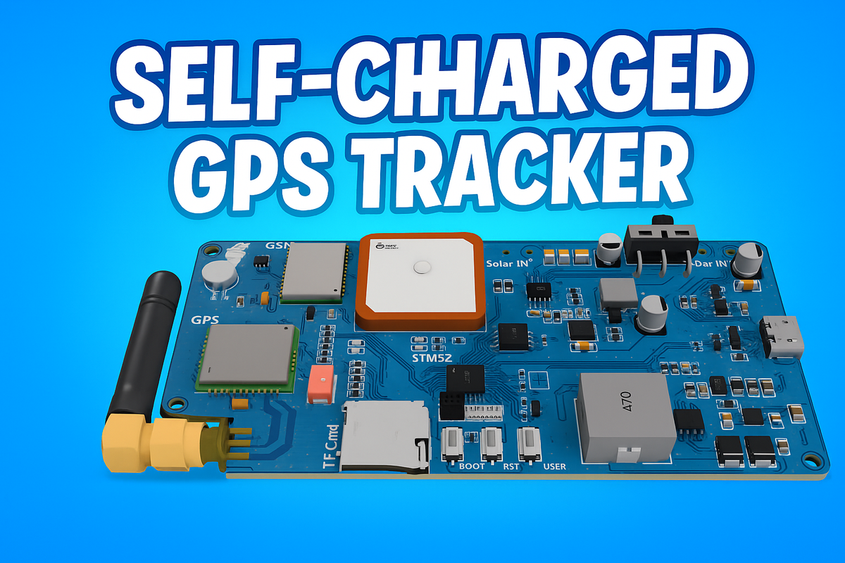
In this project, I designed and implemented a 6 x 11 cm printed circuit board (PCB). The primary goal of this board is to build a GPS tracking device powered by a rechargeable lithium battery, which is charged by a small 6V, 100 mA solar panel. The board is designed using only two layers to minimize manufacturing costs while maintaining performance and reliability. The device is designed to be practical for continuous tracking applications, with low power consumption that allows the battery to operate for as long as possible.
Board Features and Overall Design
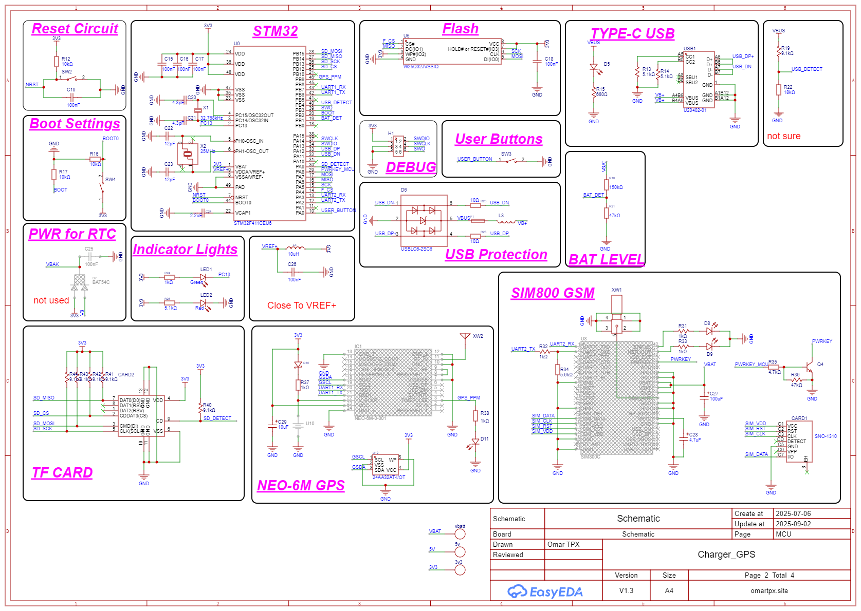
The PCB was carefully designed to minimize noise and ensure signal integrity. Connection paths were carefully considered to avoid interference between the power circuits and sensitive signal circuits, such as the GPS module. The board is equipped with a SIM800 GSM communication module, which enables data transmission via cell towers, allowing the current location to be periodically sent to a server or mobile phone. The board also includes a NEO-6M GPS module, which provides accurate, real-time coordinates.
A smart, adjustable charging circuit is included, allowing the charging current or tracking voltage to be adjusted according to the requirements of the system or the solar panel being used. Additionally, the board is equipped with multiple protection circuits against reverse current, overcurrent, and overcharging and overdischarging of the battery.
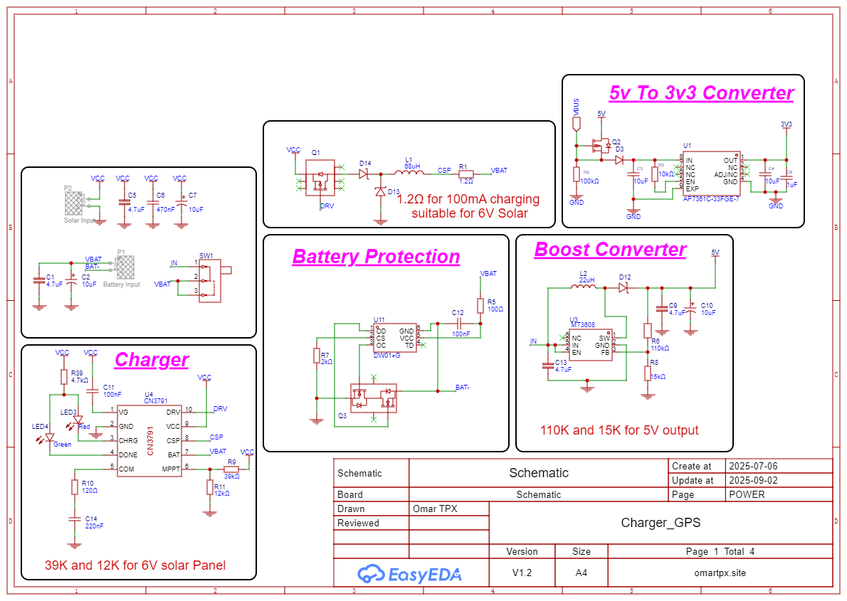
The power circuit is built around the CN3791, an MPPT charging module for solar panels. Auxiliary components such as the DW01+G were added to protect the battery, the MT3608 to step up the voltage to 5V, and the AP7361C low-noise voltage regulator was used to convert the voltage to 3.3V needed to power the STM32 and other modules. Other components such as the CEM4435A MOSFETs, additional resistors, and capacitors were carefully selected to ensure stable circuit operation.
Main Components of the System
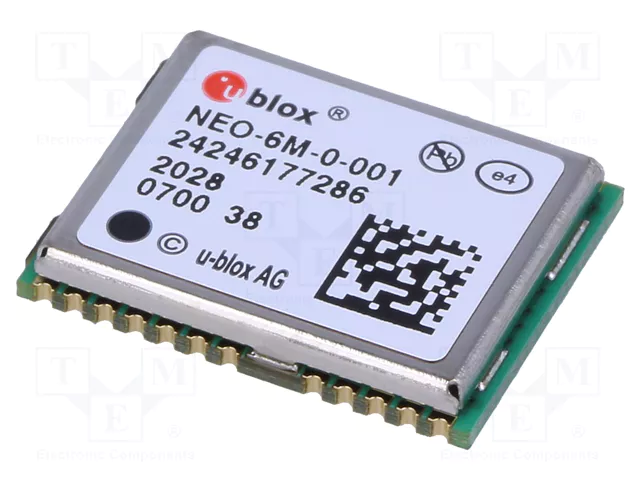
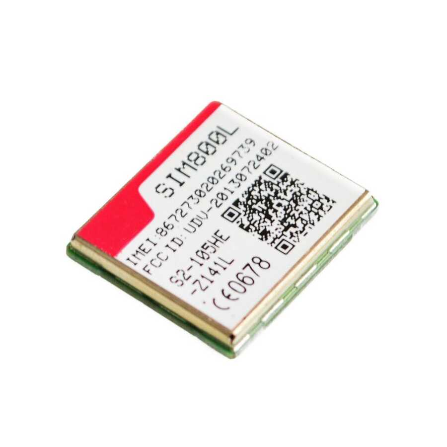
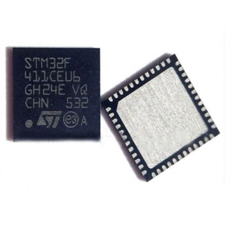
The main processor is an STM32, which controls all components. It features low power consumption and sufficient processing power to control the GPS and GSM modules, read data, and store it on a TF card when needed. The NEO-6M GPS module is responsible for accurate geolocation. The GSM SIM800 module is responsible for connecting to the network and sending data to the user. Additionally, the project is supported by the ability to record data on a TF card if the location needs to be stored locally.
Power Circuit and Components
CN3791 (Solar Lithium Battery Charger with MPPT) Module
This module is responsible for charging the lithium battery using the power generated by the solar panel. What distinguishes it is that it supports Maximum Power Point Tracking (MPPT) technology, which allows the solar panel to be used more efficiently by operating at its optimal voltage. The operating point is determined by dividing the resistors connected to the MPPT port.
In this design, resistors with values of 39 kΩ and 12 kΩ were used to adjust the tracking voltage to match the 6-volt solar panel.
The equation for calculating the tracking voltage is taken from the datasheet as follows:

Where VREF = 1.205V. Using R1 = 39kΩ and R2 = 12kΩ results in a tracking voltage close to the ideal voltage for a 6V solar panel. This ensures highly efficient charging.
The CEM4435A MOSFET transistor
was used to control the charging current supplied to the battery. The resistor value used with this module determines the charging current. In this project, a 1.2 ohm resistor was used, resulting in a charging current of approximately 100 mA.
The charging current equation is as follows:
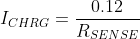
At R = 1.2Ω the charging current is close to 100mA which is consistent with the solar panel used.
MT3608 (Boost Converter) Module
It boosts the battery voltage from 3.7 volts to 5 volts. The output of this module is determined by a voltage divider resistor network, and the output equation is:
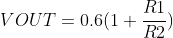
By choosing R1 = 110kΩ and R2 = 15kΩ, the output is about 5V. Although the 3.3V output could be used directly, adding an LDO was preferred to obtain a cleaner and more stable output for the STM32 processor, which requires a low-noise voltage.
AP7361C (LDO Regulator)
This module is a low-noise 3.3V voltage regulator. Its primary function is to convert the 5V output to a stable 3.3V to power the STM32 and other modules. The choice of an LDO instead of a buck converter in this case was due to the low noise and the importance of stability with the microprocessor.
DW01+G (Battery Protection IC)
Its task is to protect the battery from dangerous conditions such as overcharging, overdischarging, or drawing a current above the permissible limit. This module works in conjunction with external MOSFETs to isolate the battery in the event of an unsafe condition.
USBLC6 (USB ESD Protection)
It is used to protect the circuit from electrostatic shock (ESD) when connecting or disconnecting the USB port. A fuse is also added to the USB input for additional protection.
Additional Protection Components
A PMEG6030 Schottky diode was used to prevent reverse current when the battery and USB port are connected together. Another DMG3415 MOSFET was added to create an ideal diode circuit that minimizes voltage loss during switching.
PCB Design
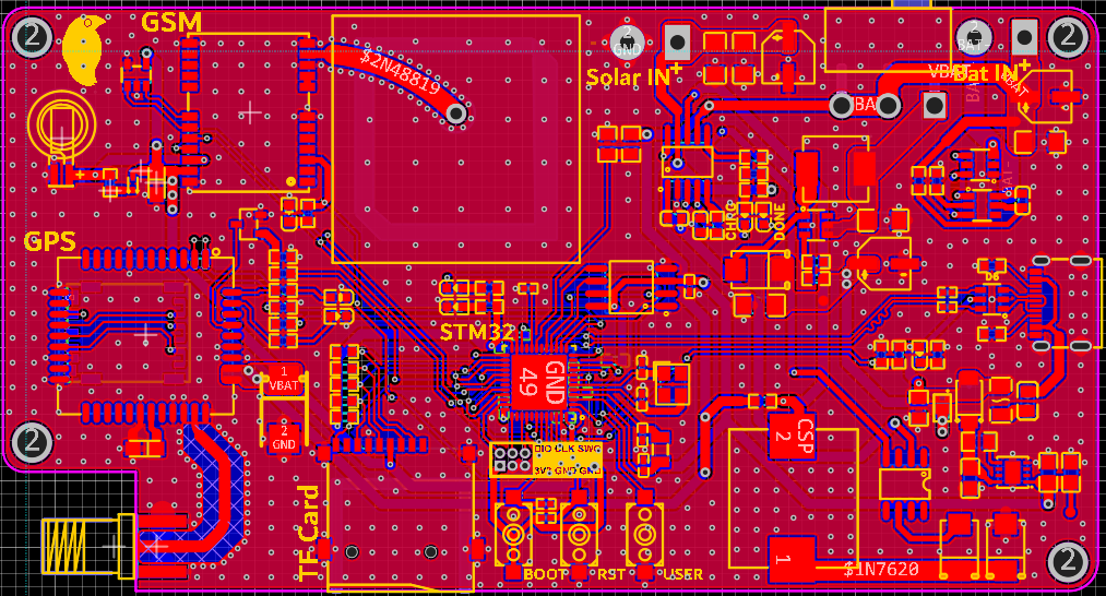
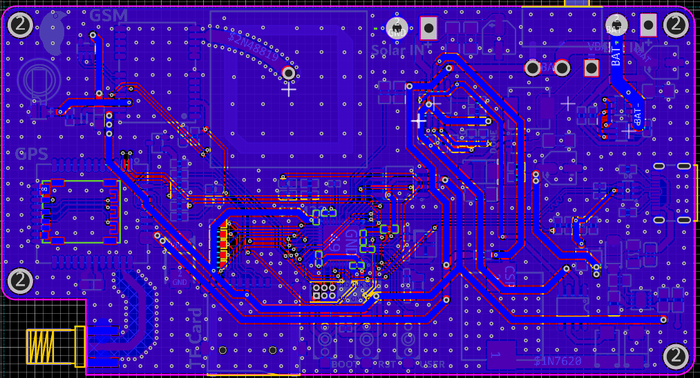
The board is designed in two layers. An entire section is dedicated to the power circuit, containing all components for charging, conversion, and battery protection. This section includes detailed notes in the schematic to explain how to modify the circuit's performance when changing the solar panel specifications or when increasing the charging current. For example, when using a higher-current solar panel, the resistor connected to the CEM4435A can be adjusted to increase the charging current.
For the CN3791 section, MPPT-specific resistors were selected according to the equation in the datasheet to set the voltage to 6 volts. For the MT3608 section, the calculated resistors were used to output 5 volts. Although the resistors could have been adjusted to output 3.3 volts, the reason for this is that the LDO is more efficient at handling sensitive signals and ensuring a stable voltage.
Also, when designing the 5V to 3.3V converter section using the AP7361C, it was taken into account that the voltage drop caused by current passing through the PMEG6030 diode and the DMG3415 MOSFET does not affect the performance of the voltage regulator, as the drop is very small compared to the regulator input.
BOM and Gerber Files
Firmware and Software Implementation
The STM32 microcontroller serves as the main controller that orchestrates all peripherals connected on the PCB. Each pin is assigned to a specific hardware function, and the firmware must configure these pins correctly during initialization before entering the operational loop. Below is a full description of how the firmware will manage each subsystem based on the provided connections.
1.SD Card Interface (PB15, PB14, PB13, PB12, PA9)
The SD card is connected over the SPI bus using the following mapping:
- PB15 – MOSI (Master Out Slave In): Data sent from the STM32 to the SD card.
- PB14 – MISO (Master In Slave Out): Data received from the SD card.
- PB13 – SCK (Serial Clock): SPI clock driven by the STM32.
- PB12 – CS (Chip Select): Used to select the SD card device. Active low.
- PA9 – SD_DETECT: Detects if the SD card is physically inserted.
The firmware initializes the SPI peripheral in mode 0 (CPOL = 0, CPHA = 0), at a moderate frequency (~400 kHz during initialization, then increased up to 18 MHz for data transfer). The FATFS library is mounted once the SD_DETECT pin confirms card presence. If no card is detected, logging is disabled but transmission over GSM remains functional.
2.GPS Interface (PB7, PB6, PB9)
The NEO-6M GPS module is connected to UART1:
- PB7 – UART1_RX: Receives NMEA sentences from the GPS module.
- PB6 – UART1_TX: Transmits configuration commands to the GPS module (optional, e.g., to change baud rate or sentence output).
- PB9 – GPS_PPM: Pulse-per-second output from GPS, used for precise timing if needed.
The firmware initializes USART1 at 9600 baud, 8N1 (default for NEO-6M). Data reception is interrupt-driven: each received character triggers an interrupt and is stored in a circular buffer. Once a full NMEA line ending with \r\n is received, the parsing routine is executed.
The $GPRMC or $GPGGA sentences are parsed for:
- UTC time
- Latitude and longitude (converted to decimal degrees)
- Fix status
- Number of satellites
- Altitude (optional)
If the GPS_PPM pin (PB9) is enabled, it can generate a precise 1 Hz interrupt for synchronization, ensuring the system timestamps logs accurately.
The FATFS implementation uses standard file I/O operations (f_open, f_write, f_sync, f_close) so logs can be easily accessed on a PC.
3. GSM Interface (PA3, PA2)
The SIM800 GSM module is connected to UART2:
- PA3 – UART2_RX: Receives responses from SIM800.
- PA2 – UART2_TX: Sends AT commands to SIM800.
The firmware initializes USART2 at 115200 baud, 8N1 (typical for SIM800, though configurable). The STM32 implements an AT command driver:
- Send command string (
AT+CSQ,AT+CMGF,AT+CMGS, etc.) - Wait for response string within timeout
- Compare response against expected acknowledgment (
OK,ERROR) - Return result to higher-level GSM handler
The higher-level GSM handler supports:
- Sending SMS with location data
- Optional GPRS connection (TCP/IP) for sending data to a server
- Signal quality checking
- Automatic retry if network is not available
The SIM800 is powered down between transmissions to reduce consumption, controlled via GPIO.
4. Power and Battery Monitoring (PB1, PB4)
- PB1 – BAT_DET: Connected to a resistor divider that scales down battery voltage for safe ADC input. The ADC reads the scaled voltage, which the firmware converts back to the real battery level using the divider ratio. This allows continuous monitoring of battery status.
- PB4 – USB_DETECT: Detects when the device is powered by USB. When USB is plugged in, the firmware may switch operation mode (for example, enabling debugging logs over UART or writing continuously to SD card without worrying about battery consumption).
The battery management algorithm uses thresholds:
- Low threshold → reduce transmission frequency, disable GSM
- Critical threshold → keep only GPS active, log locally, and avoid GSM usage
- Normal threshold → allow full operation with logging and GSM transmission
5. User Interface (PA0)
- PA0 – USER BUTTON: Configured as an input with external interrupt. It can be used for several functions:
- Manual trigger for immediate GPS + GSM transmission
- Entering special debug/test mode
- Forcing system reset
Debounce is handled in software with a short delay (~50 ms) after detection.
6. Firmware Main Loop
After initialization, the firmware runs in a low-power event-driven loop:
- Check SD_DETECT (PA9): If SD card is inserted, mount FATFS.
- Wake up GPS (PB6/PB7, PB9): Acquire coordinates.
- Log Data: Write timestamp, GPS fix, battery voltage into log file.
- Wake up GSM (PA2/PA3): Transmit data via SMS or GPRS.
- Power Down GSM: Save energy.
- Check Battery Voltage (PB1): Adjust duty cycle based on charge level.
- Enter Sleep Mode: Until next scheduled wake-up or user button press.
Interrupts (UART RX for GPS/GSM, EXTI for user button, EXTI for SD_DETECT) ensure the system remains responsive while consuming minimal power.
Example Code Skeleton
int main(void) {
    SystemClock_Config();
    MX_GPIO_Init();
    MX_USART1_UART_Init();   // GPS
    MX_USART2_UART_Init();   // GSM
    MX_SPI1_Init();          // SD card
    MX_ADC1_Init();          // Battery voltage

    FATFS fs;
    if (HAL_GPIO_ReadPin(SD_DETECT_GPIO_Port, SD_DETECT_Pin) == GPIO_PIN_RESET) {
        f_mount(&fs, "", 1); // Mount SD if present
    }

    while (1) {
        gps_get_fix(&gps_data);       // From NEO-6M via UART1
        battery_voltage = read_battery(); // From PB1 ADC

        log_to_sd(&gps_data, battery_voltage);

        gsm_send_data(&gps_data, battery_voltage);

        enter_low_power_mode(); // Sleep until next cycle
    }
}
Project Images
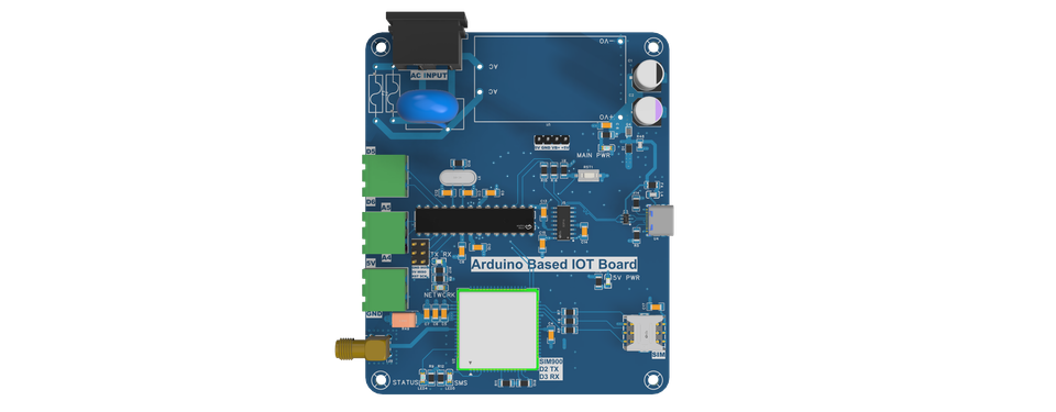
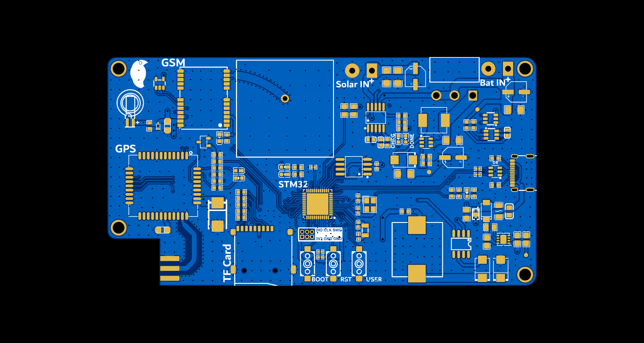
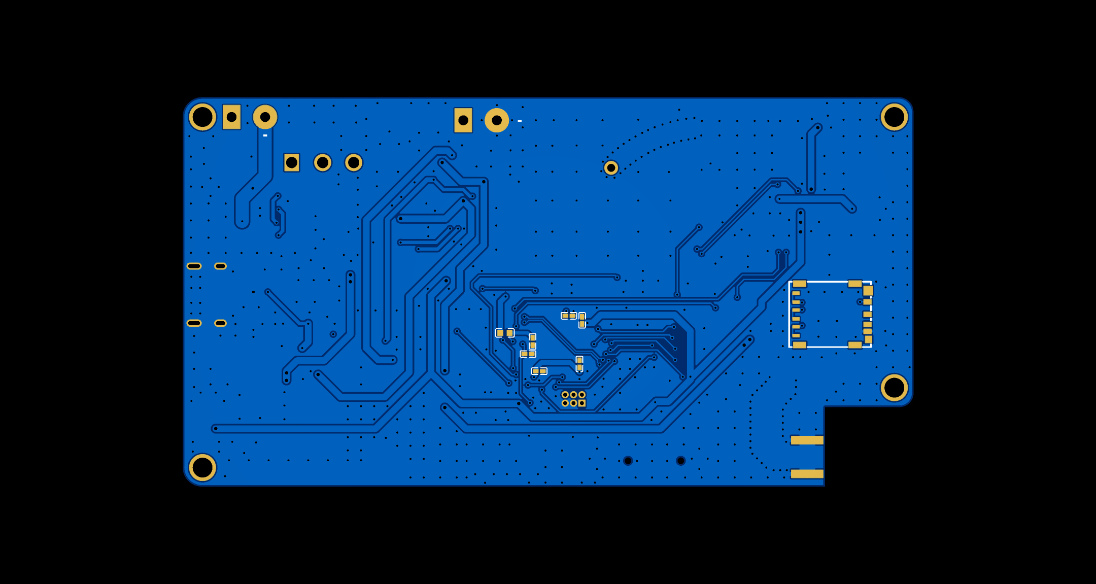
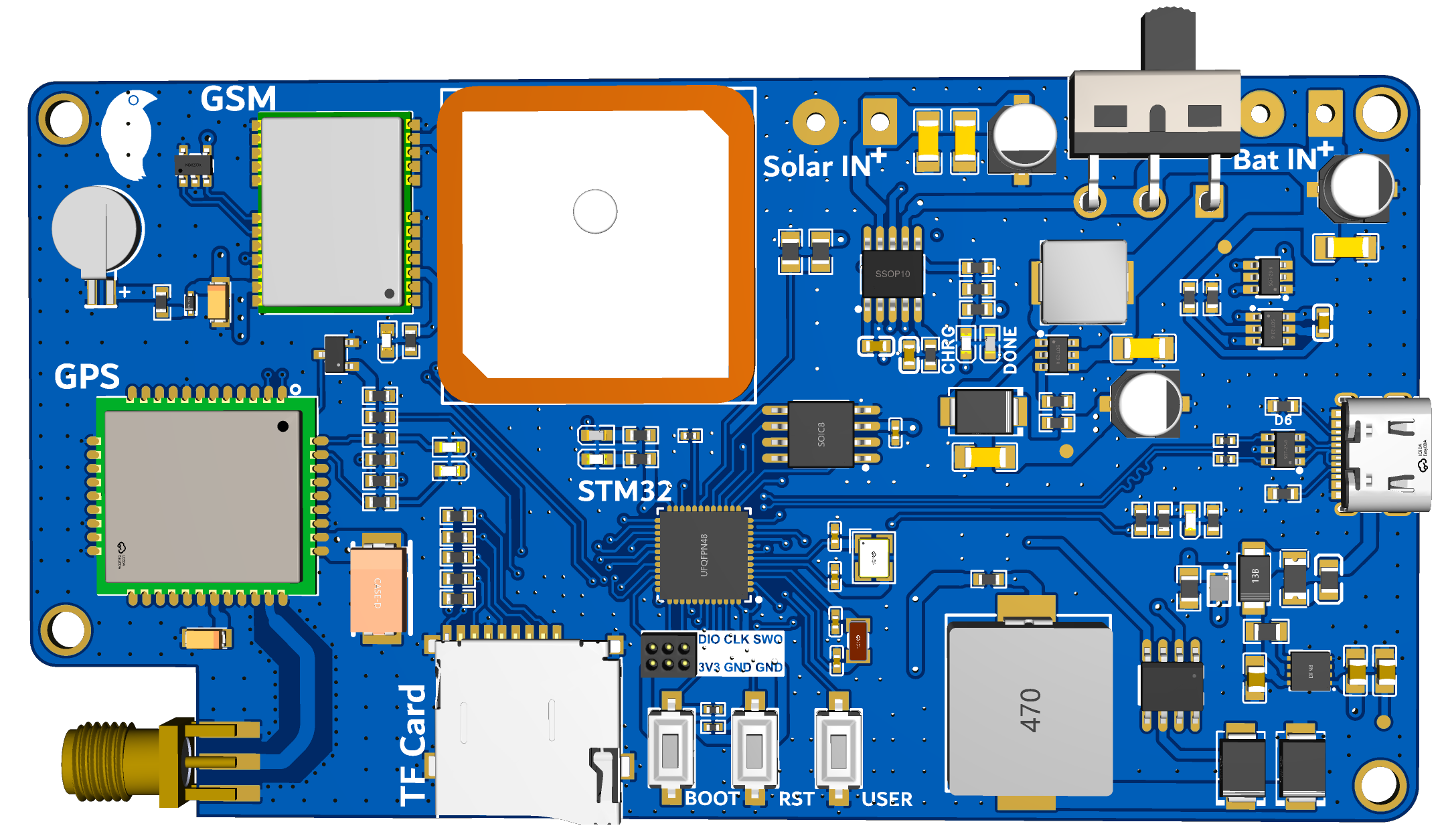
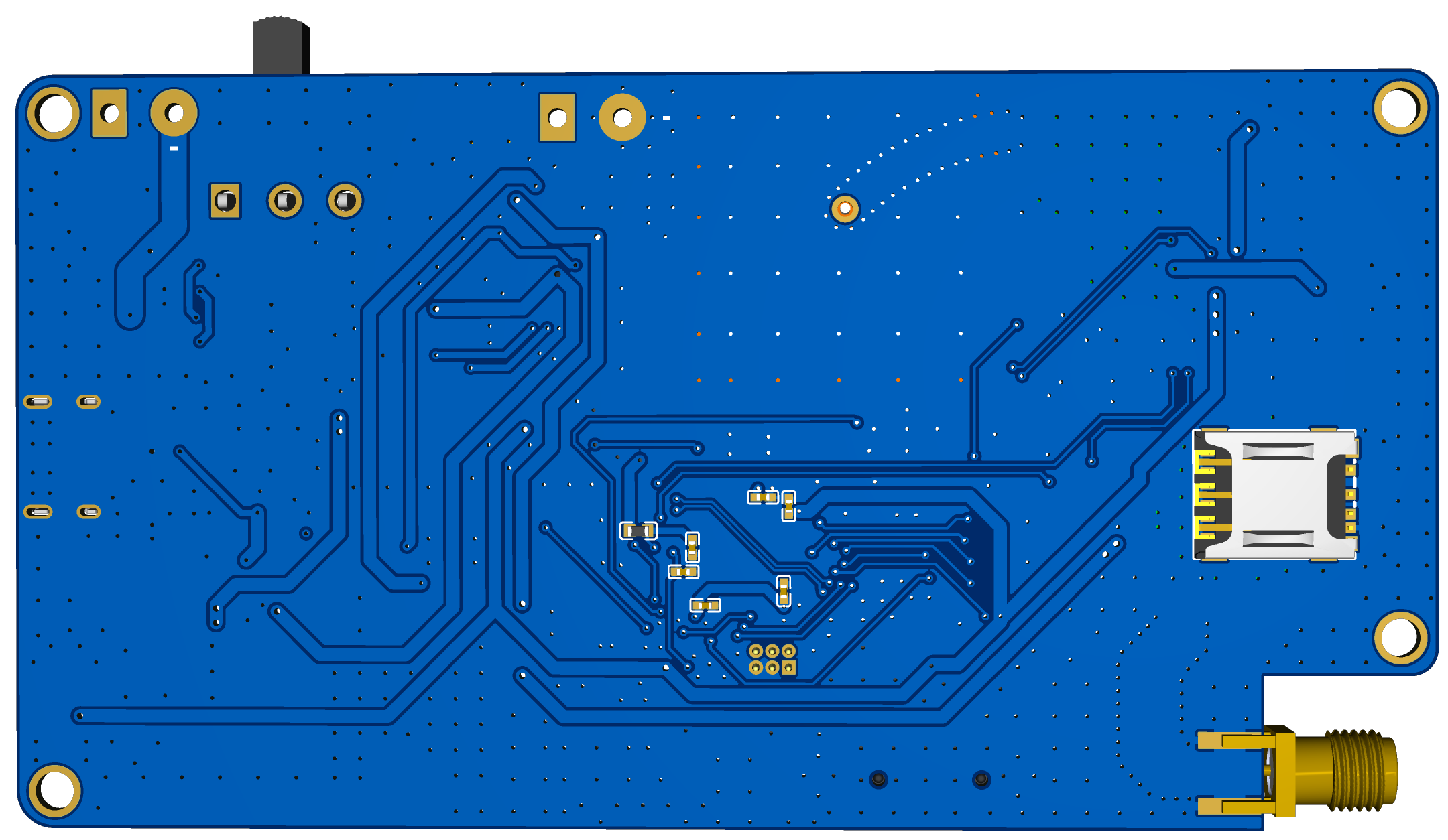
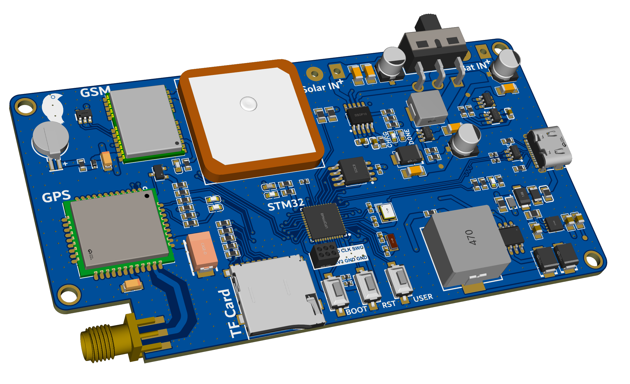
3D and 2D renderings of the PCB were created to illustrate the expected final appearance of the board, as well as a PCB layout showing the distribution of components and paths.
Summary
By mapping the peripherals directly to STM32 pins, the firmware architecture is now tied to the hardware design:
- SPI1 (PB15, PB14, PB13, PB12) → SD card logging with FATFS
- USART1 (PB7, PB6, PB9) → GPS acquisition and timing
- USART2 (PA3, PA2) → GSM communication with AT command driver
- ADC (PB1) → Battery monitoring
- GPIO (PB4, PA0, PA9) → USB detect, user button, SD detect
This mapping ensures that once the PCB is fabricated and components are soldered, the firmware can directly control every module without further changes. The modular software design allows you to later expand features, such as switching from SMS to TCP/IP, adding encryption, or using the GPS_PPM signal for high-precision timestamping.
I haven't yet had the opportunity to order this board, purchase all the components, and assemble the project, nor have I been able to write the STM32 software. However, the complete schematic and design are ready for use, and when the project is physically implemented, I will share the development step-by-step, from assembly to performance testing and writing the software needed to control the module and send data.